Class information for: |
Basic class information |
| Class id | #P | Avg. number of references |
Database coverage of references |
|---|---|---|---|
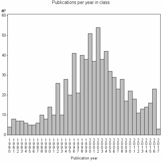
| 14198 | 785 | 17.0 | 65% |
Hierarchy of classes |
The table includes all classes above and classes immediately below the current class. |
| Cluster id | Level | Cluster label | #P |
|---|---|---|---|
| 2 | 4 | MATERIALS SCIENCE, MULTIDISCIPLINARY//PHYSICS, APPLIED//PHYSICS, CONDENSED MATTER | 2836879 |
| 279 | 3 | SELF ASSEMBLED MONOLAYER//MOLECULAR ELECTRONICS//NANOSCIENCE & NANOTECHNOLOGY | 42929 |
| 482 | 2 | ATOMIC FORCE MICROSCOPY//ATOMIC FORCE MICROSCOPE//AFM | 15691 |
| 14198 | 1 | SCANNING CAPACITANCE MICROSCOPY//SSRM//INSYS | 785 |
Terms with highest relevance score |
| rank | Term | termType | Chi square | Shr. of publ. in class containing term |
Class's shr. of term's tot. occurrences |
#P with term in class |
|---|---|---|---|---|---|---|
| 1 | SCANNING CAPACITANCE MICROSCOPY | authKW | 672333 | 4% | 52% | 33 |
| 2 | SSRM | authKW | 605179 | 3% | 68% | 23 |
| 3 | INSYS | address | 272432 | 5% | 19% | 36 |
| 4 | SCANNING CAPACITANCE MICROSCOPE | authKW | 238243 | 1% | 88% | 7 |
| 5 | CARRIER PROFILING | authKW | 233383 | 1% | 100% | 6 |
| 6 | SCANNING SPREADING RESISTANCE MICROSCOPY SSRM | authKW | 200041 | 1% | 86% | 6 |
| 7 | DIAMOND TIPS | authKW | 155589 | 1% | 100% | 4 |
| 8 | SCANNING CAPACITANCE MICROSCOPY SCM | authKW | 155581 | 1% | 50% | 8 |
| 9 | SCANNING SPREADING RESISTANCE MICROSCOPY | authKW | 146606 | 1% | 54% | 7 |
| 10 | CARRIER SPILLING | authKW | 116691 | 0% | 100% | 3 |
Web of Science journal categories |
| Rank | Term | Chi square | Shr. of publ. in class containing term |
Class's shr. of term's tot. occurrences |
#P with term in class |
|---|---|---|---|---|---|
| 1 | Physics, Applied | 10698 | 73% | 0% | 575 |
| 2 | Nanoscience & Nanotechnology | 6950 | 32% | 0% | 251 |
| 3 | Engineering, Electrical & Electronic | 3778 | 41% | 0% | 323 |
| 4 | Microscopy | 1272 | 4% | 0% | 35 |
| 5 | Materials Science, Coatings & Films | 851 | 8% | 0% | 62 |
| 6 | Physics, Condensed Matter | 641 | 17% | 0% | 131 |
| 7 | Materials Science, Multidisciplinary | 155 | 13% | 0% | 103 |
| 8 | Instruments & Instrumentation | 120 | 5% | 0% | 37 |
| 9 | Materials Science, Characterization, Testing | 114 | 2% | 0% | 13 |
| 10 | Electrochemistry | 112 | 4% | 0% | 30 |
Address terms |
| Rank | Term | Chi square | Shr. of publ. in class containing term |
Class's shr. of term's tot. occurrences |
#P with term in class |
|---|---|---|---|---|---|
| 1 | INSYS | 272432 | 5% | 19% | 36 |
| 2 | MAT COMPONENTS ANAL GRP | 116691 | 0% | 100% | 3 |
| 3 | CORP NANO DEVICES | 51862 | 0% | 67% | 2 |
| 4 | C A S | 38897 | 0% | 100% | 1 |
| 5 | COMPONENTS TECHNOL | 38897 | 0% | 100% | 1 |
| 6 | CORP NANODEVICES | 38897 | 0% | 100% | 1 |
| 7 | CREAT INITIAT SCI NANOMETER SCALE | 38897 | 0% | 100% | 1 |
| 8 | CREAT SCI NANOMETER SCALE | 38897 | 0% | 100% | 1 |
| 9 | CRISMAT LAMIPS COMMUN ENSICAENUMR CNRS 6508 | 38897 | 0% | 100% | 1 |
| 10 | CRISMAT NXP SEMICOND | 38897 | 0% | 100% | 1 |
Journals |
| Rank | Term | Chi square | Shr. of publ. in class containing term |
Class's shr. of term's tot. occurrences |
#P with term in class |
|---|---|---|---|---|---|
| 1 | JOURNAL OF VACUUM SCIENCE & TECHNOLOGY B | 68532 | 22% | 1% | 171 |
| 2 | MICROELECTRONICS RELIABILITY | 5015 | 4% | 0% | 30 |
| 3 | APPLIED PHYSICS LETTERS | 3237 | 12% | 0% | 97 |
| 4 | MICROELECTRONIC ENGINEERING | 2967 | 4% | 0% | 28 |
| 5 | SOLID-STATE ELECTRONICS | 2238 | 3% | 0% | 24 |
| 6 | INSTITUTE OF PHYSICS CONFERENCE SERIES | 1727 | 3% | 0% | 21 |
| 7 | SOLID STATE TECHNOLOGY | 1685 | 1% | 0% | 9 |
| 8 | MATERIALS SCIENCE IN SEMICONDUCTOR PROCESSING | 1411 | 1% | 0% | 11 |
| 9 | JOURNAL OF THE ELECTROCHEMICAL SOCIETY | 1046 | 4% | 0% | 29 |
| 10 | ULTRAMICROSCOPY | 983 | 2% | 0% | 12 |
Author Key Words |
Core articles |
The table includes core articles in the class. The following variables is taken into account for the relevance score of an article in a cluster c: (1) Number of references referring to publications in the class. (2) Share of total number of active references referring to publications in the class. (3) Age of the article. New articles get higher score than old articles. (4) Citation rate, normalized to year. |
| Rank | Reference | # ref. in cl. |
Shr. of ref. in cl. |
Citations |
|---|---|---|---|---|
| 1 | OLIVER, RA , (2008) ADVANCES IN AFM FOR THE ELECTRICAL CHARACTERIZATION OF SEMICONDUCTORS.REPORTS ON PROGRESS IN PHYSICS. VOL. 71. ISSUE 7. P. - | 95 | 46% | 82 |
| 2 | CLARYSSE, T , VANHAEREN, D , HOFLIJK, I , VANDERVORST, W , (2004) CHARACTERIZATION OF ELECTRICALLY ACTIVE DOPANT PROFILES WITH THE SPREADING RESISTANCE PROBE.MATERIALS SCIENCE & ENGINEERING R-REPORTS. VOL. 47. ISSUE 5-6. P. 123 -206 | 56 | 81% | 25 |
| 3 | LANYI, S , (2010) ON THE LATERAL RESOLUTION OF SCANNING CAPACITANCE MICROSCOPE BASED C-V MEASUREMENTS.ULTRAMICROSCOPY. VOL. 110. ISSUE 10. P. 1343-1348 | 28 | 97% | 0 |
| 4 | WILLIAMS, CC , (1999) TWO-DIMENSIONAL DOPANT PROFILING BY SCANNING CAPACITANCE MICROSCOPY.ANNUAL REVIEW OF MATERIALS SCIENCE. VOL. 29. ISSUE . P. 471 -504 | 30 | 97% | 151 |
| 5 | KIMURA, K , KOBAYASHI, K , YAMADA, H , MATSUSHIGE, K , USUDA, K , (2006) TWO-DIMENSIONAL CARRIER PROFILING ON OPERATING SI METAL-OXIDE SEMICONDUCTOR FIELD-EFFECT TRANSISTOR BY SCANNING CAPACITANCE MICROSCOPY.JOURNAL OF VACUUM SCIENCE & TECHNOLOGY B. VOL. 24. ISSUE 3. P. 1371-1376 | 30 | 86% | 5 |
| 6 | CHANG, MN , HU, CW , CHOU, TH , LEE, YJ , (2012) CONTRAST DISTORTION INDUCED BY MODULATION VOLTAGE IN SCANNING CAPACITANCE MICROSCOPY.APPLIED PHYSICS LETTERS. VOL. 101. ISSUE 8. P. - | 21 | 88% | 2 |
| 7 | LANYI, S , (2008) SHAPE DEPENDENCE OF THE CAPACITANCE OF SCANNING CAPACITANCE MICROSCOPE PROBES.ULTRAMICROSCOPY. VOL. 108. ISSUE 8. P. 712-717 | 25 | 81% | 0 |
| 8 | GIANNAZZO, F , RAINERI, V , MIRABELLA, S , BRUNO, E , IMPELLIZZERI, G , PRIOLO, F , (2005) SCANNING CAPACITANCE MICROSCOPY TWO-DIMENSIONAL CARRIER PROFILING FOR ULTRA-SHALLOW JUNCTION CHARACTERIZATION IN DEEP SUBMICRON TECHNOLOGY.MATERIALS SCIENCE AND ENGINEERING B-SOLID STATE MATERIALS FOR ADVANCED TECHNOLOGY. VOL. 124. ISSUE . P. 54-61 | 25 | 83% | 3 |
| 9 | DUHAYON, N , CLARYSSE, T , EYBEN, P , VANDERVORST, W , HELLEMANS, L , (2002) DETAILED STUDY OF SCANNING CAPACITANCE MICROSCOPY ON CROSS-SECTIONAL AND BEVELED JUNCTIONS.JOURNAL OF VACUUM SCIENCE & TECHNOLOGY B. VOL. 20. ISSUE 2. P. 741-746 | 21 | 100% | 18 |
| 10 | YANEV, V , ROMMEL, M , BAUER, AJ , FREY, L , (2011) CHARACTERIZATION OF THICKNESS VARIATIONS OF THIN DIELECTRIC LAYERS AT THE NANOSCALE USING SCANNING CAPACITANCE MICROSCOPY.JOURNAL OF VACUUM SCIENCE & TECHNOLOGY B. VOL. 29. ISSUE 1. P. - | 17 | 89% | 0 |
Classes with closest relation at Level 1 |