Research
Programmable Photonic Computing |
||
|
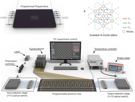
We demonstrate how synthetic gauge fields for light can be engineered on a 12-mode programmable photonic processor using discretized Floquet evolution. We observe hallmark signatures of topological transport: chiral photon circulation that flips with drive inversion, flux-controlled interference with high visibility, and robust directional flow in multi-site lattices. |
 |
arxiv: 2509.13184 |
|
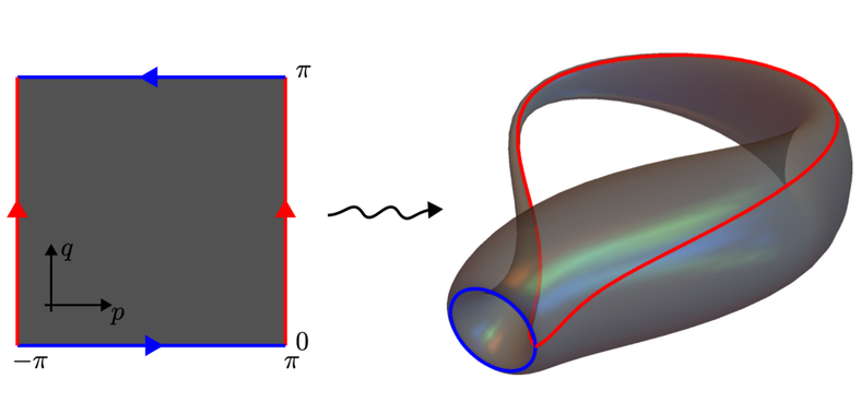
We demonstrate a scalable photonic emulation of non-Hermitian topology by realizing a two-band Hamiltonian defined on a non-orientable Klein-bottle parameter space using a programmable silicon photonic processor. The observed Fermi arc orientation reveals a nontrivial exceptional topology with same-charge exceptional points that cannot locally annihilate, constituting the first photonic realization of exceptional monopole physics on a non-orientable manifold. |
 |
arXiv:2512.20273 |
|
We demonstrate programmable coherent absorption of quantum light by implementing tunable non-unitary transformations on an integrated linear photonic circuit using ancilla-mode dilation. By emulating a lossy beam splitter with full control over phase, transmission, reflection, and absorption, we observe phase-dependent switching between perfect transmission and deterministic single-photon absorption, as well as nonlinear-like behavior for two-photon NOON states, including photon bunching and probabilistic two-photon absorption. |
 |
arXiv:2510.02541 |
Hybrid Quantum Photonics |
||
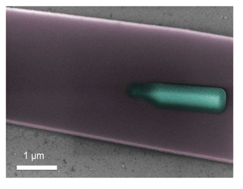
| We developed a hybrid process for integrating high quality single photon emitters in a CMOS compatible platform. The process is deterministic in terms of selecting the quantum emitter, using a nano-manipulator, and the design of the photonic circuit. The developed hybrid platform exploits the advantages of high quality single-photon sources grown on III-V platforms with well-developed silicon based photonics. | 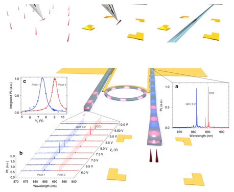
|
Nature Communications 8, 379 (2017)
|
 |
Nano Lett. 16 (4), 2289–2294 (2016) | |
 |
Nature Photonics, 14, 285-298 (2020), Review paper | |
| We develop a site-controlled process to deterministically integrate 2D quantum emitters in silicon nitride photonic waveguides. The hybrid integration methods allows to intrdouce quantum light sources to photonic platforms with no inherent light emitting properties. hBN is an exciting quantum material with potential with capability of emitting single light particles with high quantum efficiency at room temperature , without the need of extreme refrigiration. |  |
Adv. Quantum Technol., 2100032 (2021) (Journal Cover) |
|
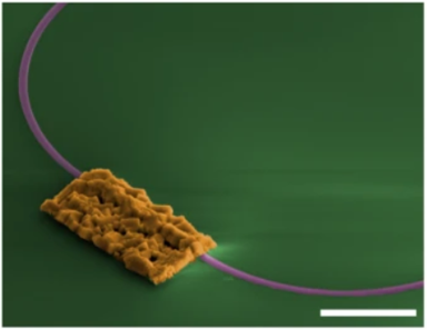
We realize a hybrid system combining site-controlled Cu2O micro-crystals and silicon nitride photonic circuits. In the work, we couple Cu2O exciton emission to a SiN waveguide, the emission shows excellent quality on par with micro-crystals grown on thermal oxide. The platform offers exciting possibilities through exploring rydberg excitons in Cu2O for strong light matter interaction, mediated by high order rydberg states in Cu2O. |
|
Topological Photonics and condensed matter physics simulations |
|
|
|
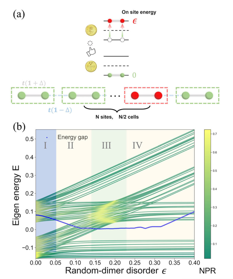
We report the first experimental observation of reentrant localization in a disordered photonic lattice. Using a photonic SSH model with correlated (random-dimer) disorder, we show that increasing disorder can unexpectedly restore extended transport after localization, revealing anomalous wave-function dynamics and highlighting integrated photonics as a powerful platform for simulating complex condensed-matter phenomena. |
|
|
|
We experimentally investigate mobility-edge physics in a quasiperiodic photonic lattice with engineered modulation. By breaking lattice duality and tuning disorder, we observe the coexistence of extended and localized states and directly probe mobility edges via single-site excitation, establishing integrated photonics as a versatile platform for exploring localization phenomena beyond standard Anderson models. |
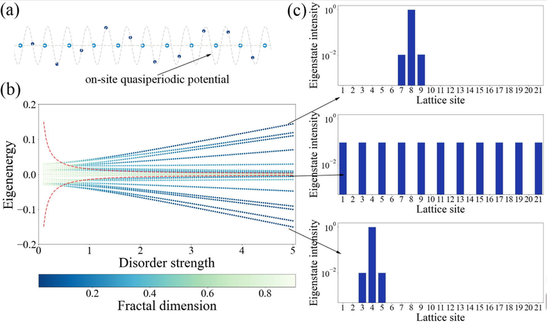 |
Science Bulletin 70 (2025) 58–63
|
|
We demonstrate a direct measurement of topological invariants in chiral photonic superlattices with broken inversion symmetry. Using a CMOS-compatible nanophotonic chip and tailored bulk excitation, we identify topological zero modes through quantized beam displacement, enabling single-shot characterization of topological phases in complex multi-band photonic systems. |
 |
Photon. Res. 10(12), 2901-2907 (2022) (Editor Pick)
|
|
We experimentally observe a topological Anderson phase in a disordered photonic lattice, where disorder induces protected edge states in an otherwise trivial system. Using a CMOS-compatible nanophotonic implementation of the SSH model, we directly track edge-state dynamics and demonstrate a disorder-driven inverse transition between distinct topological phases. |
 |
Strain-tunable Quantum Photonics |
||
| We developed a strain-tunable hybrid quantum photonic platform by integrating silicon nitride waveguides with preselected III-V nanowire QDs on a piezoelectric substrate. An applied electric field tunes both the emitter wavelength and ring resonator frequency via strain. The device is stable and bonding-free, making it ideal for atomic memory integration. | 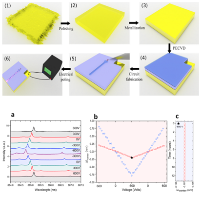 |
Nano Lett. 18 (12), 7969-7976 (2018) |
| We successful transfer of a nanowire quantum dot onto a luthium niobate. The emission of the nanowire QD can be dynamically controlled by creating an acousto-optical interaction with surface acoustic waves. The single photon source retains its purity even during the process of dynamics strain tuning. | 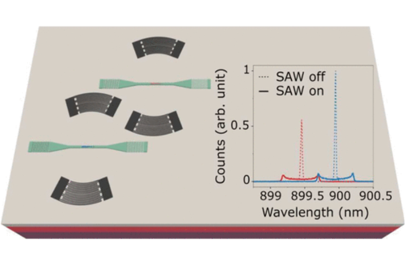 |
|
| ACS Photonics 10 (10), 3691–3699 | ||
|
We realize low-power microelectromechanical reconfiguration of integrated photonic circuits interfaced with superconducting single-photon detectors on the same chip. |
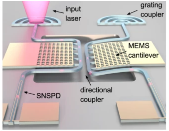 |
Nature communications 12 (1), 1408 |
Quantum Entanglement |
||
|
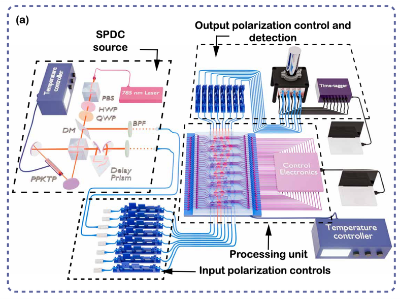
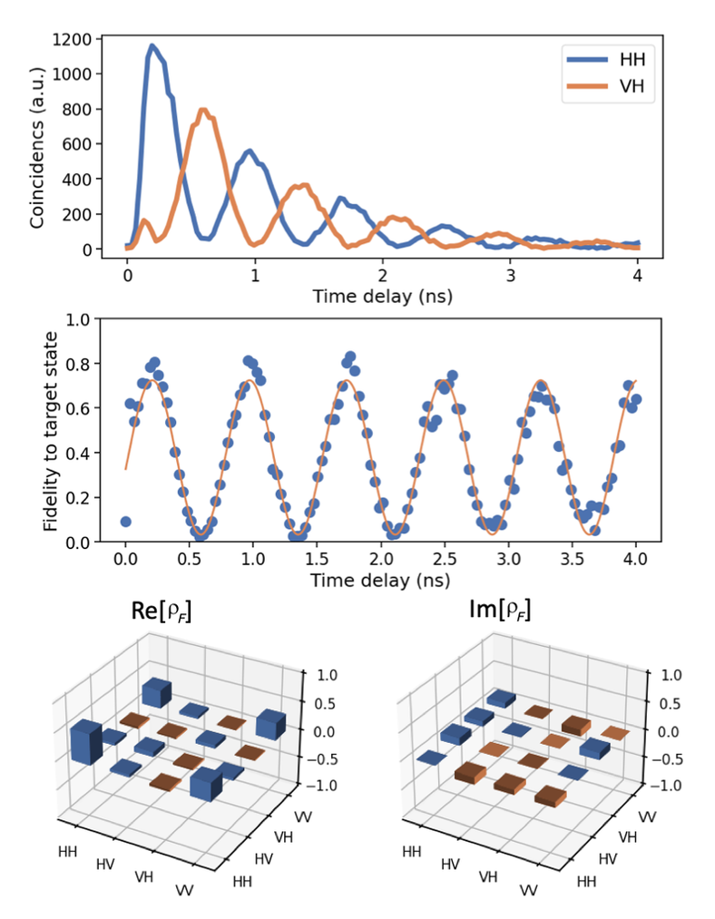
We demonstrate a reliable and scalable technique for geenrating and reconstructing the W state in photonic circuits using Fourier and real-space imaging, supported by the Gerchberg-Saxton phase retrieval algorithm. We utilize an entanglement witness to distinguish between mixed and entangled states, thereby affirming the entangled nature of our generated state. |
|
|
| We demonstrate bright entangled photon pair generation in the telecom O-band using site-controlled nanowire quantum dots, achieving 85.8% fidelity and 75.1% concurrence, enabling scalable quantum networks. |  |
Nano Lett. 2025, 25, 26, 10321–10327 |
|
We demonstrate Fourier-transform quantum state tomography for polarization-encoded photonic qubits, enabling full state reconstruction using only a single rotating waveplate per qubit. The method scales linearly with system size and accurately characterizes single- and two-qubit states from quantum dots and SPDC sources, with fidelities matching conventional projective tomography. |
 |
arXiv:2503.18311 |

Lidar |
||
|
We demonstrate a photon-counting LIDAR system based on thermal light with engineered oscillating photon bunching, enabling high-precision ranging without active signal modulation. By operating a sub-threshold laser at telecom wavelengths and spectrally filtering its emission, we generate an enhanced, oscillatory second-order correlation function that increases the effective bunching and signal-to-noise ratio. |
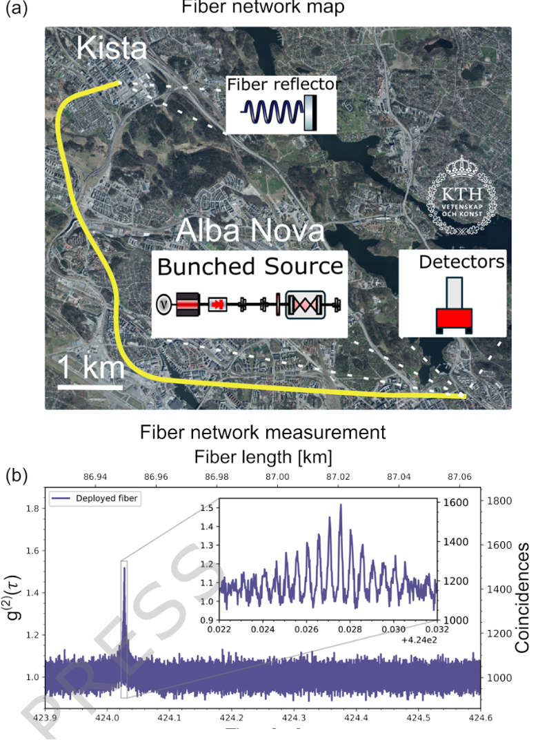 |
nature communicatons |
|
We demonstrate single-photon LIDAR architectures based on frequency-modulated continuous-wave (FMCW) and time-of-flight detection using superconducting nanowire single-photon detectors. |
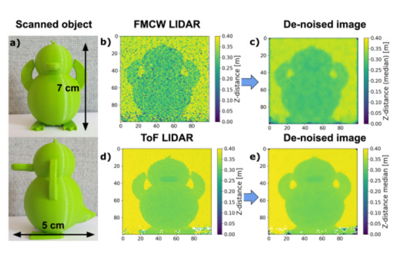 |
Opt. Express 32, 7332-7341 (2024)
|
Superconducting Single Photon Detectors |
||
|
Superconducting nanowire single-photon detectors (SNSPDs) are a key technology for quantum photonics, offering high detection efficiency, low dark counts, and picosecond timing resolution. Ongoing research in this area focuses multiplexing and wavelength sensitivity. |
 |
APL Photonics 5, 111301 , (2020) (Featured Article)
Nano Letters 23 (21), 9748-9752
Nanophotonics 12 (3), 339-358 (Review)
|
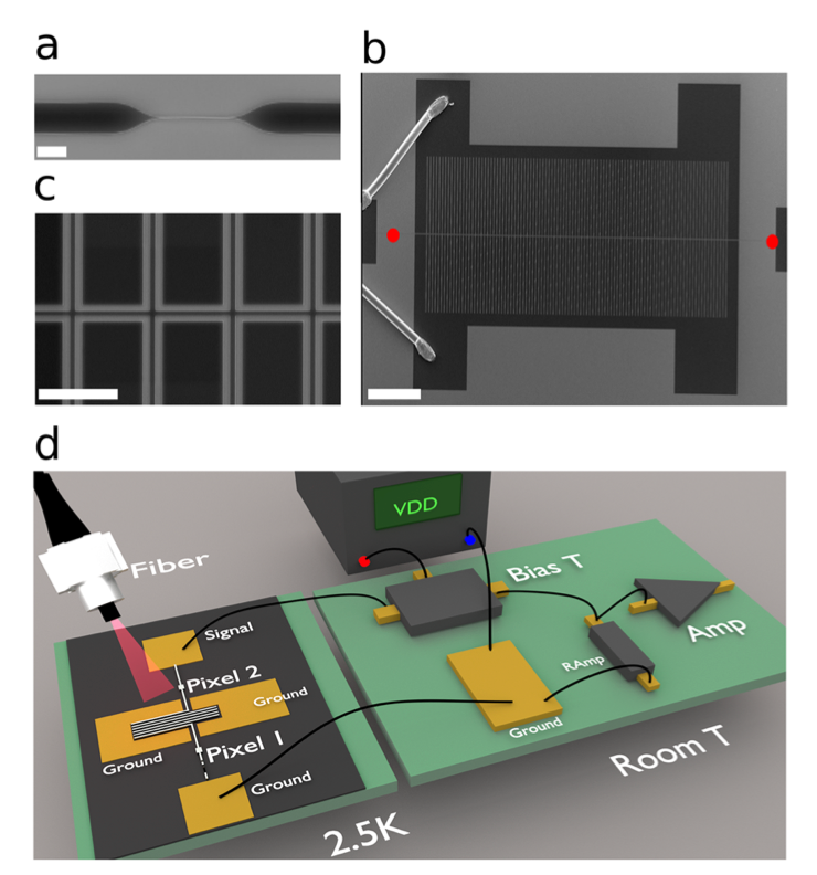
| We realize a fully integrated, proof of concept, quantum channel, combining nanowire single photon emitter, a silicon nitride waveguide, and a ring resonator filter terminated with a single photon detector. | 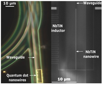 |
Optics Express 27(17), 24601-24609 (2019) |
Single photon wavelength conversion |
||
|
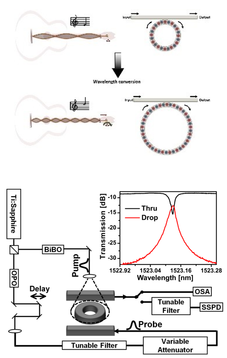
We investigate the theoretical and experimental dynamic tuning of optical resonators and its effect on trapped single photons. Like adjusting a guitar string’s tension mid-note, tuning the cavity alters the photon’s frequency. This shift is linear within the adiabatic regime. |
 |
Appl. Phys. Lett. 101, 171110 (2012)
Phys. Rev. A 82, 063839 (2010)
Optics Express 27, 14400-14406, (2019)
|
Photonic-Analogue of Electromagnetically-Induced Transparency |
||
| On-chip optical buffers are challenging in silicon photonics due to loss from carrier-based tuning. We experimentally demonstrated a carrier-free optical storage element using a photonic analogue of Electromagnetically Induced Transparency (EIT). By dynamically tuning coupled microcavities, we created a supermode that enables controllable storage and release of light pulses. | 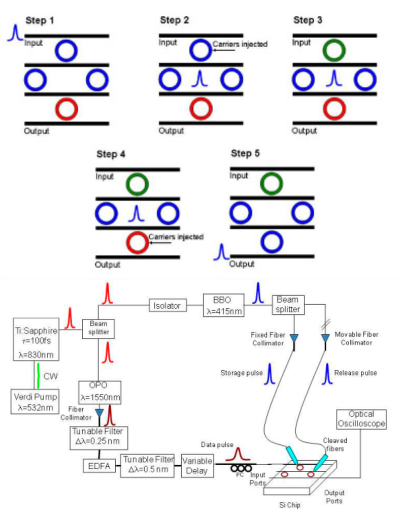 |
Optics Express 18 (3), 3014-3022 (2010)
|
Material Properties Characterization |
||
| Accurate material characterization is vital for photonic circuit design. We measured the thermo-optic coefficients of PECVD SiN and SiO₂ at cryogenic temperatures, essential for quantum applications. At room temperature, the coefficients are 2.51 ± 0.08 × 10⁻⁵ K⁻¹ (SiN) and 0.96 ± 0.09 × 10⁻⁵ K⁻¹, both decreasing by an order of magnitude at 18 K, offering key insights for low-temperature photonic device design. | 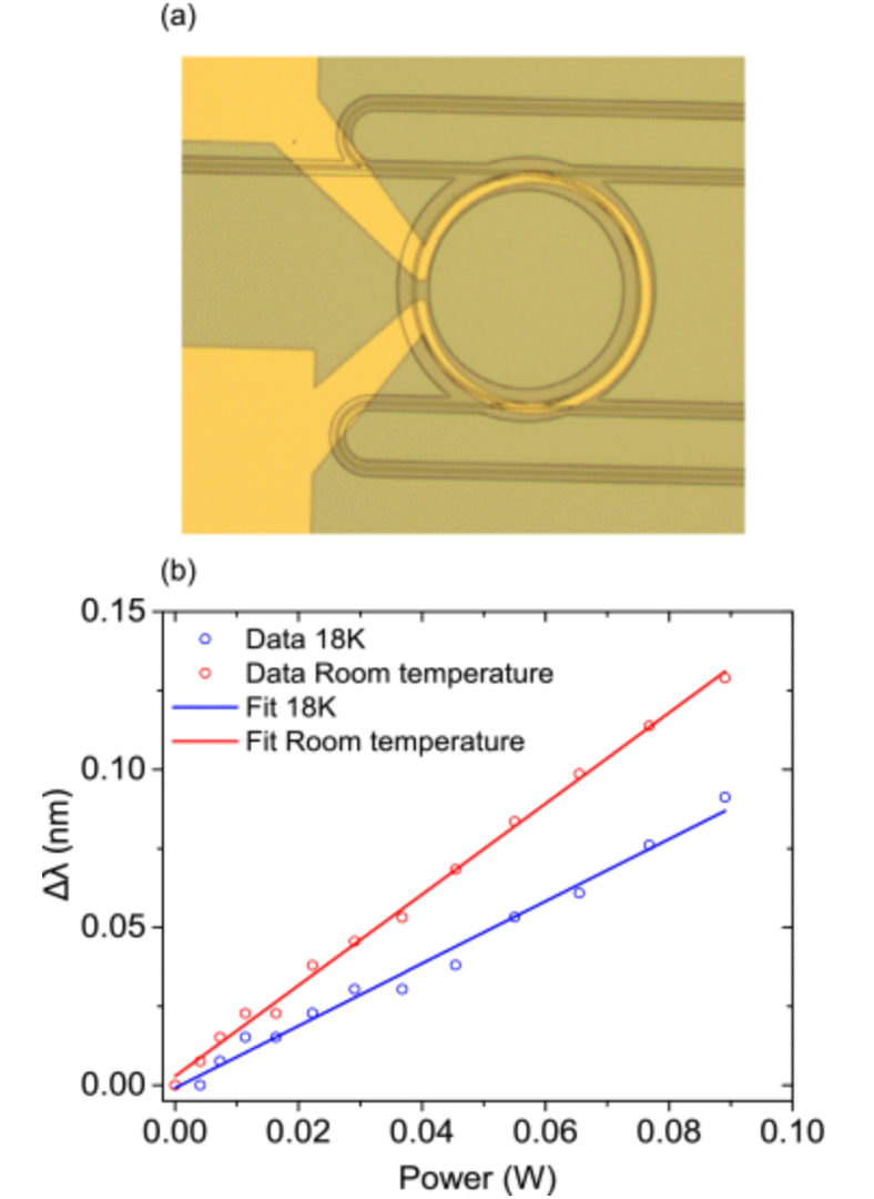 |
IEEE Photonics, 8 (3), 2701009 (2016) |