

Former Nano silicon Group
The "Nano silicon" group performed research on advanced silicon micro and nano fabrication technologies and nanostructures including silicon nanowires, silicon nanocrystals – quantum dots and structured scintillators for X-ray imaging. The group included 15-20 PhD students and postdocs over the years. Group Head was Professor Jan Linnros.
Example research projects were:
Silicon Nanocrystals
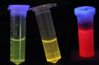
Silicon nanocrystals can be fabricated by various techniques such as ion implantation, CVD deposition or by lithography, etching and oxidation or by chemical methods. When the diameter reaches below ~5 nm quantum confinement sets in and a quantum dot is formed. This results in efficient, size-tunable emission that could potentially be used for displays, as a phosphor or for labelling bio molecules. We are currently investigating the light emission mechanism and the physics of Si quantum dots using single-dot spectroscopy, quantum yield…
Silicon nanowires
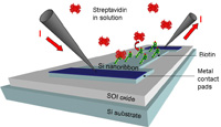
Silicon nanowires can be used for electrical detection of bio molecules. This is because the conductance of a tiny nanowire is very sensitive to surface charges. Thus, the nanowire surface is functionalized with receptor molecules that bind specifically to a certain bio molecule. As bio molecules are often charged, binding involves charge transfer which can be detected as a change in the nanowire conductance. Using a 45 nm thick ‘nanoribbon’ we recently showed a sensitivity of about 20 bio molecules……
Silicon nanofabrication including electrochemical etching
The ultimate goal is silicon handcrafting at a nanometre level where quantum physics come into play and where silicon acquires new characteristics. The methods we use are conventional silicon processing (in the Electrum clean room laboratory) combined with electron-beam lithography. Oxidation is then a key process for shrinking dimensions in a controlled way. We are also studying high-aspect ratio etching either by DRIE (Deep Reactive Ion Etching) or by electrochemical etching. This results in arrays of deep pores which can be used for X-ray imaging (see below), for membranes or, as recently discovered, for creating surfaces with super hydrophobic properties……
Scintillator arrays for X-ray imaging
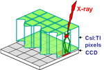
X-ray imaging detectors usually have a scintillating layer converting X-rays to visible photons as detected by a CCD or CMOS detector. In our patented design, the scintillator is structured into pores which provide efficient light guiding to the detector pixels. This concept has now been commercialised by Scint-X, a start-up company in Electrum. Here, we take this technology further by reducing the pore dimension down to the few micron level for high-lateral resolution X-ray imaging……