Visa version
Visa
< föregående
|
nästa >
Jämför
< föregående
|
nästa >
Lab1 wiki (en)

Chips and Breadboard

At the labs, we use digital circuits from the so-called 74-series of capsules of the DIL type (Dual In Line) for hole PCB assembly. See the picture. This is today considered to be pure spare parts, and development has changed to completely different package types for surface mounting.
These old circuits, are however unbeatable for experiments with simple connections on the breadboard. Breadboard are now also used with very complex circuits - then mounted on Breakout Board (a breakout board has the same pin spacing DIL) circuits. Working with circuits on the breadboard is therefore the natural working method for project work and theses for school and hobby activities.
Fritzing Is the name of a software for documenting breadboard connections, and generate circuit diagrams, and possibly manufacture printed circuit boards. (This program will be used in the course IE1206 but is not needed for this course). Anyone interested can download it now.
Data sheets for laboration circuits
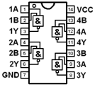
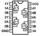
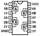
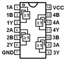
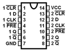
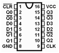
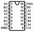
The digital components have capsules with 14 or 16 pins. For orienting the capsules they have an outlet on the short side, and there can also be a "dot" to mark the pin number 1. Two of the pins should be connected to the supply voltage and ground and the other pins are used as logic inputs and outputs, sometimes a pin can lack connection to the inside of the chip, it is then called NC (no Connection). The pin function is stated in the data sheets, and to some extent also in the symbols in the figures.
Some warnings.
Two outputs may not be connected with each other. It will be a so-called short-circuit and the output value becomes uncertain 1/0 (?). Unconnected inputs picks up electrical interference and must therefore also be considered unsafe 1/0 (?). They should therefore always be connected to an appropriate fixed level 1/0 depending on the function.
Breadboard
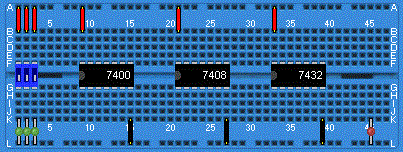
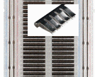
Breadboard at the lab. Supply voltage and ground are already connected to circuitry on the labequipment. To the right is a picture of the coupling underside of the deck with the contact springs visible, and a picture of a contact spring for five holes.
Breadboard at the lab. The chips are inserted in the holes on the plastic isolated side. On the underside there are contact springs of metal that electrically connects to the pins and for further connection to four additional holes. Connector cables can then be entered in the holes to pass on the connection to other pins.
The contact springs are in groups of five holes vertically. This corresponds to a connection point (a node) in a wiring diagram. In the middle of the breadboard is an insulating "ditch" so that the pins on the chips both long sides are isolated from each other. Coupling on long sides of the board have extra long contact springs, so that all the holes are here connected to each other. The long side holes are used to connect the supply voltage and ground to the other circuits. Upper long side holes are all connected to + 5V and lower long side to ground (0V).
Many breadboard has double rows of holes on the long sides - each side of the board can then have both the supply voltage and ground. Then you can avoid having to draw cables over the chips, this facilitates in the case that one chip fails and must be replaced.
Long breadboards often has long side contact springs divided into two sections and two rows. The sections can then be used for several different supply voltages to the circuits - no standard for this does exist - for such a case, you simply carefully has to find out what applies!
Other components
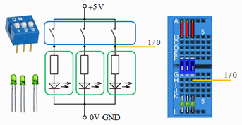
To generate the logical input signals we use DIP switches and green LEDs. Note that we are using special LEDs with built-in current limiting resistors (they cost a penny more, but simplifies the circuit)! When the switch is open, the logic signal is 0 on the yellow line, because the LED is off and keeps the wire at 0V. When the switch is closed, it is supplying current to the green LED, the voltage is + 5V, and the LED lights, and the logic signal on the yellow wire is then 1. You operate the DIP-switch with a screwdriver tip.
![]()
To se the logic circuitry output levels, we use red LEDs.
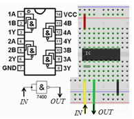
From schematic to breadboard conection.
In the diagram we have a NAND gate connected as inverter. In reality, on the breadboard we have to select one of the four NAND gates in the chip. A jumper (gray jumper wire) connects the two inputs together. Yellow wire IN leads to the input and the green line OUT to the gate output. Supply voltage (red line) and ground (black wire) is also connected to the chip.
Simulation of logic functions
- Can we check logic functions without having to connect circuits?
The original way to verify that the electronic costructions are functioning as intended was to hook them up and then make control measurements on the circuit. As electronics became more complex and integrated, this has become difficult - while computer programs have been developing so that it is now natural to rely on simulations.
1973 the simulation program SPICE (Simulation Program with Integrated Circuit Emphasis) was developed of the University of California, Berkeley, for use in the design of integrated electronic circuits. It is this program that is still used today by electronics designers - and we use a more modern version, LTSpice, in this course!
Spice is an analog simulator, it thus uses continuous values of voltages and currents. This is necessary for those who will design integrated circuits, but to show logic functions we could be content with a simpler simulator that only expects 1 and 0. The computational power of today's PCs are so high that we do not have to choose!
Visit: http://www.linear.com/ to download and install the program LTspice on your own computer. You do not need to register if you do not want to. The installation is then "straightforward" as described on the website. The program is available for most operating systems, but this tutorial describes the appearance under Windows.
Course simulation files
The program is installed on school computers in lab Ka-305 and in computer room Ka-309. In school you have to unzip the course simulation files in your server folder as H:\IE1204 . (at home you can unzip the files in any folder place).
You start LTSpice by doubleclick on any  *.asc - file.
(You can also start the program ![]() LTSpice from the start menu).
LTSpice from the start menu).
 If you click on the simulation icon in the program a simulaton will start with the settings we have choosen for you. Then you can simply proceed by changing values and other preferences to explore all the course circuits!
 IE1204.zip all course simulation files.
A first simulation with LTSpice
We use LEDs with built-in resistors - what is it and why? We take the help from the simulator LTSpice to understand this! At the same time, we examine how to draw circuit diagrams, and simulate a circuit.
Make an electronic schematic
Make an electronic schematic with a lightdiode!
![]()
![]() Start LTspice. File - New Schematic
Start LTspice. File - New Schematic
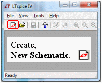
At school computers it is then important to save files in your server folder H:\
You get the components from the Edit - menu. Or if they already exists from the Shortcut menu.
![]()
Important! The Ground symbol 
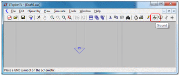
Choose component type, place, click, press <esc> when you no longer want to continue to place the same component.
To rotate the component press Ctrl-R.
![]() Every schematic must have a ground symbol GND. Place it at the first so it not will be forgotten. This is absolutely necessary - no simulations work otherwise!
Every schematic must have a ground symbol GND. Place it at the first so it not will be forgotten. This is absolutely necessary - no simulations work otherwise!
Voltage source
Then we need a voltage source (a battery). It is available in component libraries![]() opens component window. In the text box, you can search for all components, the component name is voltage but it can be enough to write the first letters vo.. for it to be found.
opens component window. In the text box, you can search for all components, the component name is voltage but it can be enough to write the first letters vo.. for it to be found.
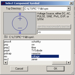
Place thevoltage source with the mouse, click and then press <esc>. The voltage source has the label/name V1 and the value/model V.
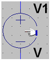
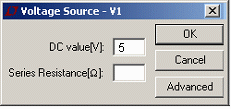
![]() To change a component, now the voltage source, move the mouse over the symbol V1 so that it assumes the shape of a hand - right click and fill in the parameter DC value [V] to 5. Now we have a 5V battery.
To change a component, now the voltage source, move the mouse over the symbol V1 so that it assumes the shape of a hand - right click and fill in the parameter DC value [V] to 5. Now we have a 5V battery.
 Diode
Diode
![]() A diode is in the component libraries. In the text box search the component name diode (dio .. could be enough). Then place the diode in the schematic.
A diode is in the component libraries. In the text box search the component name diode (dio .. could be enough). Then place the diode in the schematic.
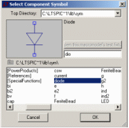
In the schematic the diode has the label/name D1 and the value/model D.


We could not use any common diode - we need a LED (Light Emitting Diode), and such model is not the supplied by the program (?) (Ordinary diodes are made from silicon, the LEDs are made of gallium arsenide - the differences in data are big, not just that the LED emits visible light!).
Now, usually, most providers of electronics publish SPICE models for their components, so after a bit of searching, we have found the following model for a LED (we are not here concerned about what the different parameters mean):
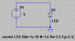
.model LED D(Is=1e-19 N=1.6 Rs=2.5 Eg=2.1)
First move the mouse pointer to the D1 model name D so that it assumes the shape of the letter I, right click and replace the model D against any other name - eg. LED. Next, we must describe the model LED for the simulator. It can easiest be done by entering the model as a SPICE directive directly somewhere on the schematic.
![]() Choose SPICE directive on the Edit menu. Copy and paste the model text from the above. (Note that the initial “point” belongs to the directive!) Click OK, and then place the text on some empty place on the schematic.
Choose SPICE directive on the Edit menu. Copy and paste the model text from the above. (Note that the initial “point” belongs to the directive!) Click OK, and then place the text on some empty place on the schematic.

![]()
(For long model texts or if you have many model descriptions it becomes unwieldy with the text directly in the schematic, then they could be placed in text files with extension *.lib.)
Wires
![]() Click on Wire. Draw lines by clicking at the start, at every bend and at the endpoint. Finish with <Esc>.
Click on Wire. Draw lines by clicking at the start, at every bend and at the endpoint. Finish with <Esc>.
![]() Move. Maybe you need to move the components, or the texts?
Move. Maybe you need to move the components, or the texts?![]() Cut. Maybe you have to delete some faults to start over?
Cut. Maybe you have to delete some faults to start over?
Simulation
Spice simulation are of many different types. Transient (time sweep), AC Analyses (frequency sweep), DC sweep, Noice, DC Transfer, DC op pnt. For the laboration preparations you will need to use Transient and DC op pnt.
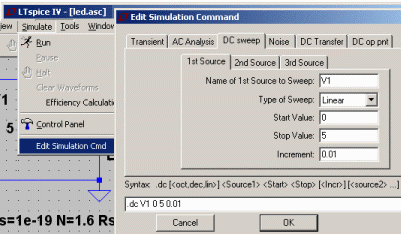
Under the Simulate menu, Edit Simulation Cmd, you can set what simulation to be done.
Under the tab DC sweep we specify that the source V1 will change linearly from 0V up to 5V in steps of 0,01V (increment). We will then be able to see how the current through the diode changes at different voltages – we will not, however, see if the LED lights (such a fun simulator is it not).
Click on OK, and place the simulation command on schematic. (An experienced user could write any simulation command directly without going through the menu Edit Simulation Cmd).
![]()
Simulate, Waveform viewer
![]()
![]()
![]() Run. Simulate by clicking on the simulate icon.
Run. Simulate by clicking on the simulate icon.
![]() Waveform Viewer is shown
Waveform Viewer is shown
| Move the mouse to any wire, then it takes the form of a voltage probe – left-click to select to display the voltage with the waveform viewer | |
| Move the mouse to any component, then it takes the form of a current probe – left-click to select to display the current with the waveform viewer. |
![]()
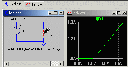
Now move the mouse to the diode symbol and left-click when it changes to a current probe. Now, the diode current will be displayed in the waveform viewer.
We can see that the relationship between voltage and current of the diode is non-linear (with a "knee" at 1.5V). When the diode is connected to a 5V power supply, the current is 1.3A, 1300 mA. Normal current for a small LED is 11.5 mA. The current is then 100 times too high when the LED is connected directly to 5V! The LED can not withstand this (100 times the current) – this it is nothing the simulator shows – but it is something that a trained engineer should still understand. (Sure it would have been fun with sound effects and animations, but remember that the simulator originates from the 1970s!).
Leave the simulation by closing the Waveform window
- LEDs must have series resistors to limit the current to the desired value. We use LEDs with integrated resistor - what value should this resistor have?
![]() Cut away some wires to make way for a resistor.
Cut away some wires to make way for a resistor. ![]() place the resistor.
place the resistor.
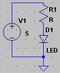

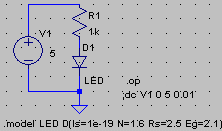
![]() Move the mouse over R at R1 so that the pointer assumes the shape of the letter I – right click and fill in the window Enter new Value for R1 to eg. 1000 (1000 ohm, can also be written 1k).
Move the mouse over R at R1 so that the pointer assumes the shape of the letter I – right click and fill in the window Enter new Value for R1 to eg. 1000 (1000 ohm, can also be written 1k).
Simulate menu, Edit Simulation Cmd, click on the tab DC op pnt. Click on OK and place the text in the schematic.
The previously simulation command has now received a semicolon in front of it (= commented out). Now the command is .op. This is the simplest simulation type, we will only get a text list of voltages and currents in the circuit.
       --- Operating Point ---

V(n002): 1.58402    voltage
V(n001): 5          voltage
I(D1):   0.00341598 device_current
The current through the LED is apparently 3.4 mA – we want to 11.5 mA (according to information in the data sheet) – so we can reduce the value of R1. Do so and simulate your way to a reasonable value. Enter this value of the series resistor in the preparations for Lab1. We can now assume that there is a similar resistance that is built into our LEDs.
It is now so common with LEDs so that some websites have adopted a script to calculate the series resistor. You can try the Online series resistor calculator (use this value for forward voltage Vf = 2.1 V).
- If you have had major problems to draw this schematic, here we have it ready made as
 ledx.asc among the course simulation files. Dubble click on that file and then simulate with
  Run.
Run.
Simulation of combinational circuits - logic gates truth tables (for the lab Combinatorial circuits)
NAND-gate 7400
Test connections to examine a NAND gate in the lab combinatorial circuits.
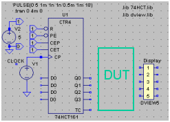
To simulate the truth tables for the combinational circuits, we have made some template files. The combinatorial circuit should be placed within the circled green area in the figure, the DUT (Device Under Test). What is needed is binary coded input signals, and such can be obtained from a "counter" that counts in binary code (We will go through the counter at the lecture 8, but start using it, 74161, already!). Q3Q2Q1Q0 counts from 0000 to 1111. In order to "scan" through the truth table they should be connected to the combinatorial network inputs.
Digital outputs is either 1 or 0, if you show them with the Waveform viewer they will all end up over one another in a non-transparent manner. Therefore we have the block DVIEW5 which displaces five digital signals separated into a clear image. There is also a DVIEW10 for up to 10 signals.
The template file contains two Spice-directive with the names of the models we need..Most of the 74-series models are in file 74hct.lib and Digital Signal Viewer models are in file dview.lib.
![]()
Open the file  truth_template2.asc and save it directly under the name
  7400_test.asc ( at school in the folder H:\IE1204\ ).
![]() Component. Top Directory Browse to the folder with the course simulation files. Then choose 74HCT00.
Component. Top Directory Browse to the folder with the course simulation files. Then choose 74HCT00.

![]() Draw wires.
Draw wires. ![]()
![]() Clean up!
Clean up!

![]() Label Net. Name the wires 1A 1B 1Y, then it becomes easier to separate the signals. Place the names at the wires (= in contact with the wire).
Label Net. Name the wires 1A 1B 1Y, then it becomes easier to separate the signals. Place the names at the wires (= in contact with the wire).

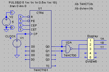
The simulation profile is this time Transient, a time sweep. The voltage source V2 is constant 5V and gives us the 0 or 1 to the circuits. The voltage source V1 is now a pulse generator which delivers 18 pulses in succession. This is more than is needed to scan through the truth table. The supply voltage for the logic circuitry is always implied by the simulator.
![]()
![]() Run. Simulate.
Run. Simulate. ![]() Waveform Viewer is shown.
Waveform Viewer is shown.
![]() Move the mouse to wire 1A and click when it changes to a voltage probe. Repeat for 1B and 1Y.
Move the mouse to wire 1A and click when it changes to a voltage probe. Repeat for 1B and 1Y.


Now insert the simulated values in the table in the lab booklet - at the lab, you will have a chance to compare them with your measured values!
- If you have had major problems to draw this schematic, here we have it ready made as
 7400_testx.asc among the course simulation files. Dubble click on that file and then simulate with
  Run.
Run.
Simulate AND-gate and OR-gate

![]()
![]()
![]() Save the file as 7408_test.asc and 7432_test.asc. Edit by switching to circuit 74HCT08 and 74HCT32
Save the file as 7408_test.asc and 7432_test.asc. Edit by switching to circuit 74HCT08 and 74HCT32
![]() Simulate and fill in the truth tables in the lab booklet. At the lab, you will have a chance to compare them with your measured values!
Simulate and fill in the truth tables in the lab booklet. At the lab, you will have a chance to compare them with your measured values!
Simulate a combinatorial circuit (Before the lab Combinatorial circuits)

Test setup for at the lab build and explore a combinatorial circuit..

Open the template file  truth_template3.asc oand save it directly under the name
  circuit_test.asc ( at school in the server folder H:\IE1204\ )
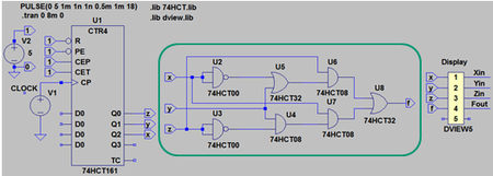
Draw the combinatorial circuit, the circled portion of the figure, and connect it to the other parts, counter and the display, so that the circuit can be simulated.
To avoid having to run wires "criss-cross" of the schematic, you can use ![]() Label Net. In addition to give a name to a point in the diagram, you can also specify it as a output or an input.
Label Net. In addition to give a name to a point in the diagram, you can also specify it as a output or an input.
![]()
An output and an input with the same name means that they are connected to each other (eg.. Z in the figure above). (Warning! two outputs can not have the same name, but several inputs can be the same).
Hint! With ![]() Duplicate you can reuse (copy, paste) things that are already on the drawing, then you don’t need to look for them in the menus.
Duplicate you can reuse (copy, paste) things that are already on the drawing, then you don’t need to look for them in the menus.
![]() Run. Simulate.
Run. Simulate. ![]() Waveform Viewer is shown.
Waveform Viewer is shown.
Enter the output values from the combinatorial circuit to the column fSIM in the truth table in the laboratory booklet as preparation task. Take the opportunity to study the timing charts - can you directly see what type of circuit this is?
Simulate the full adder (Before the lab Combinatorial circuits)

In preparation, you have reasoned your way to what the truth table must be for a full adder. Below is a circuit that is claimed to be a "full adder".

Now open the ready made file  fulladd.asc
 ![]() simulate and check the result and verify that it is consistent with your truth table. You will build the circuit and test it at the lab.
simulate and check the result and verify that it is consistent with your truth table. You will build the circuit and test it at the lab.
Compare circuits
Another way to check the circuit, is to compare it with another “perfect” full adder.
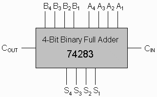
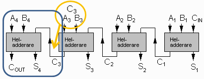
At the lab, we have the circuit 74283 that is a 4 bit adder. It consists of four full adders with a carry chain in series between them. One can not directly access all of the connections to the full adders. The fourth fulladder with Cout S4 A4 B4 has the C3 only accessible internally in the circuit.
.
You have to use a trick. If A3 and B3 are connected together so that they always have the same value, they will generate C3 because the carry out of a full adder has the same value as a majority of the input bits.
Open the ready made file  fulladd_compare.asc In the file, we are comparing the two full adder circuits for all possible inputs. The outputs are taken to two XOR gates for comparison.
![]() simulate and see if the two circuits are identical. You'll probably see some deviations, you surely want to discuss this with the lab assistants at the lab?
simulate and see if the two circuits are identical. You'll probably see some deviations, you surely want to discuss this with the lab assistants at the lab?
Full adder symmetry
What would happen if one reverses the order of the input signals to one of full adder?
In the file  fulladd_compare_crossed.asc we have done so with the wires to the circuit 74283.
![]() ssimulate and see if there is any difference. Explain the result.
ssimulate and see if there is any difference. Explain the result.
Addition of 4-bit numbers (Before the lab Combinatorial circuits)
A four-bit adder has a truth table with 256 256 (28) lines!
Should we simulate the circuit 74283 so we'll probably have be satisfied with a few test values.
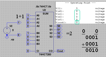
Open the ready made file  4bit_add.asc In the file we are simulating 1+1=2 (and this is obviously true).
The simulation result is a textfile with a list of voltages, and 5V means "1". You change the values by moving the mouse toward input symbol ![]() until the mouse pointer changes to I-form, then right click and change the text to the desired value..
until the mouse pointer changes to I-form, then right click and change the text to the desired value..
![]() Simulate with different numbers so that you are sure of the addition (and subtraction) of binary numbers, with and without sign.
Simulate with different numbers so that you are sure of the addition (and subtraction) of binary numbers, with and without sign.


Calculator för addition av hexadecimala tal
Multiplication with a constant (3\(\times\)) with an adder (Before the lab Combinatorial circuits)
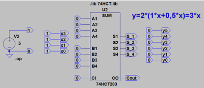
When you finished thinking about at how to multiply a 4-bit numbers x with a constant of 3 with a 4-bit adder you can try out your idea to the file  mul3_template.asc . You do not need to draw any wires it is enough to connect outputs with the inputs by editing the names.
Good luck with the lab preparations!
