CMOS Technology at KTH
- The division of Electronics and Embedded Systems at KTH has established a CMOS technology based on fully depleted silicon on insulator (FDSOI) transistors and 3 level metallization.
- The technology includes a fabrication process of CMOS wafers in KTH's Electrum Laboratory and a design kit in Cadence environment.
- The full digital design flow from HDL to GDSII is available using Cadence tools GENUS211 (digital synthesis), INNOVUS181 (digital place & route), XCELIUM1803 (digital simulation), IC618 (Virtuoso Schematic and layout editor) and PVS161 (Design rule check and layout versus schematic physical verification).
- The CMOS technology is open to any academic researchers to design and fabricate integrated circuits.
- In collaborative work, it is possible to adopt the CMOS process to integrate heterogeneous materials/devices for innovative systems.
For further inquires, please contact Per-Erik Hellström,
| KTH's FDSOI CMOS Technology | |
|---|---|
| Min gate length: | 1 µm |
| Min transistor width: | 2 µm |
| Metal 1 width/pitch | 2/4 µm |
| Metal 2 width/pitch | 2/4 µm |
| Metal 3 width/pitch | 2/4 µm |
| Supply Voltage: VDD | 1.8-2.5 V |
| Inverter propagation delay | <300 ps |
| Off-state leakage current | <1 nA/µm |
| Basic digital standard cell library | 53 Cells (NAND, NOR, INV, DFF, XOR, BUF, MUX...) with various strengths |
| Packing density (2-input NAND equivalent) | ~2500 \(gates/mm^2\) |
| Die size | 7x7 \(mm^2\) |
| Typical process time | 2 months |
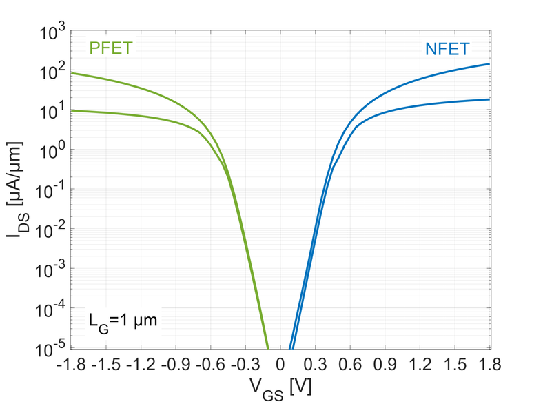 Transfer characteristics (T=25 °C) of PFET and NFET devices with minimum gate length.