Arne Quellmalz
Forskare
Detaljer
Forskare
Om mig
Arne is a researcher in electrical engineering with an interest in photonic microsystems and two-dimensional (2D) materials with a thickness on the atomic scale.
Current Research
Integration of 2D materials for high-volume semiconductor manufacturing

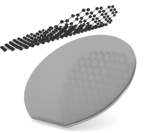
Layered materials with thicknesses on the atomic scale (2D materials) promise to revolutionize key application areas like sensing, photonics, and electronics. However, without a viable integration technology for manufacturing on industrial scale in semiconductor foundries, 2D materials will never be used beyond academic research and not deliver the great potential they hold.
The goal of this project is to mature and demonstrate a technology for integrating 2D materials with conventional semiconductor substrates, to the level needed for deployment in the production lines of semiconductor foundries. In the long-run, the activities in this project are an important steps towards the application of 2D materials in functional components, opto-electronics, and logic circuits.
Graphene photodetectors for miniaturized optical gas sensors
 Air quality is invisible and strongly affects our health and performance. In cities, it changes dramatically from one hour to the next and from one block to another. A dense mesh of mobile miniaturized sensors reporting air quality, in real time, will help us to make informed decisions and in the long run to improve air quality.
Gas sensing technologies for carbon dioxide (CO2), carbon monoxide (CO), ethanol and hydrocarbons are important for air quality monitoring, breath-based alcohol sensing, aeronautic and automotive applications as well as medical and industrial safety systems. For many of these applications existing gas sensors are too expensive, bulky or low-performance. Thus, there is a critical need for low-cost and compact gas sensor systems which are highly sensitive and specific to their targeted gas.
To address this need, we develop optical gas sensor systems utilizing mid-infrared (mid-IR) graphene photodetectors for the wavelength range from 2 to 5 µm. Existing mid-IR detectors are typically based on compound semiconductors which hinder the development of low-cost systems.
Compared to state-of-the-art optical gas sensors, our technology platform will reduce the fabrication cost to a fraction. Gas sensing systems will shrink in dimensions and potentially lower their energy consumption substantially. Integrated into mobile devices, the miniaturized sensors will provide novel features to consumer electronics in the future.
ULISSES - Gas sensors for everyone, everywhere
Short CV
Arne Quellmalz received a Ph.D. degree in Electrical Engineering from KTH Royal Institute of Technology. Thesis title: Integration of Two-Dimensional Materials for Electronics and Photonics.
In 2016, he received a M.Sc. degree in Electrical Engineering from Hamburg University of Technology (Germany). He specialized in Nanoelectronics and Microsystem Technology and performed his master thesis at RISE Acreo in Stockholm (Sweden) which is entitled "Design, Process Integration and Characterization of Silicon Nanowires for Biosensing in Lab-on-a-Chip Applications".
In 2014, he participated in an exchange program at Uppsala University and conducted a research visit at the division for Nanotechnology and Functional Materials. He contributed to a research project about nanocellulose materials for biomedical applications such as virus removal by filtration.
Besides his studies he worked part-time as working student at NXP Semiconductors in the development laboratory Protection & Filtering (BL General Applications Discretes).
Arne joined the division of Micro and Nanosystems at KTH Royal Institute of Technology in Stockholm (Sweden) in 2016. His main interest lies in photonic microsystems and two-dimensional (2D) materials with a thickness on the atomic scale.
Teaching
Microsystem Technology (EK2350)
Keywords: microsystems, nanosystems, graphene, TMDs, 2D materials, integration, transfer, photodetector, MEMS, contact resistance, sheet resistance, humidity sensitivity, bottom-contact, optical gas sensing, MIR, silicon photonics, nanocellulose, nanofiltration, size-exclusion filters,